Back to Homepage & Index

This Page - DC. to DC. Converters

Introduction
DC to DC converters are used primarily whenever it is necessary to provide specific  voltage supplies from a single primary power source and consequently they find wide application in battery powered and mains powered electronic equipment. They operate by converting the primary power source voltage to an alternating voltage suitable for transforming and rectifying to the required operating voltage(s); the voltage transformation being effected by means of capacitance or inductance (transformers and chokes). Of these the latter is by far the most widely used and which is the subject of this note. The conversion of the source voltage to an alternating voltage is achieved by switching/commutating it to a transformer or choke by electronic switches (transistors) in an oscillatory circuit; the transformer or choke being a component of the oscillator or not as the case may be. The input voltage waveform so produced is therefore a square wave. Square wave drive is used in the majority of dc to dc converter circuits, although sine wave converters are used for specific applications.
Fundamentals
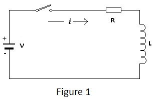
Consider the simple circuit of Figure 1 including an inductance ‘L’ Henrys, inevitable circuit resistance ‘R’ Ohms, a switch and a battery providing a source of electro-motive force (emf) of ‘V’ volts.


So far  an ‘air cored’ inductance, such as would be produced by a coil of wire of many turns wound on a plastic tube, has been assumed. For the inductance values typically used in practical DC to DC converter circuits, the number of turns necessary could result in high resistance and consequently very poor efficiency. Air cored inductors are therefore used rarely; their use being limited to high frequency applications requiring very low values of inductance (μH). More practical values of inductance (mH to H) for DC to DC converter circuits must be wound on magnetic materials , eg. iron or ferrite, if resistance is not to become a severe constraint. Figure 2B typifies what might be expected if the same number of turns had been wound on magnetic material eg. the limb of a transformer yoke. Here it can be seen that the current initially rises very slowly due to a much higher value of inductance and then suddenly rises rapidly to intercept the air-cored characteristic when the magnetic core saturates and ceases to have any effect. All magnetic materials saturate; the point of saturation for a given core assembly being a function of the core material and the product of current and the number of  turns (Ampère– turns), not time as might be concluded from the figure. The phenomenon of magnetic saturation was formerly employed in self commutating DC to DC converter circuits: the collapse of inductance, with the concomitant collapse of back emf. being used to trigger the necessary switching action. However circuits operating in this mode are comparatively inefficient. Also the operating frequency varies with the applied voltage and this, together with the noise spikes due to current surges at saturation, makes it difficult to achieve compliance with emc. regulations. Consequently saturating core converters have fallen from favour in recent times but the operating principles provide a useful starting point for discussion of DC to DC converters in general.
Discussion so far has been in terms of the back emf. produced by the rate of change of current through the winding of an inductor which equals the applied voltage in the absense of resistance. Obviously for voltage transformation up or down, a secondary winding on the magnetic core is required. Also the required voltages (both primary and secondary) are present only while the switch is closed and current is increasing. No back emf. is present if the current becomes static at a value determined by the circuit resistance prior to saturation and when the switch opens entirely different emfs. of opposite polarity are generated by the windings due to the fall of primary current. The latter property is utilised in an alternative type of DC to DC converter to be discussed but for the type currentl y being considered, no useful activity occurs during the time the switch is open; which limts the conversion efficiency. This limitation is overcome by using two primary inductors which switch on alternately in a push-pull circuit as shown in Figure 3.

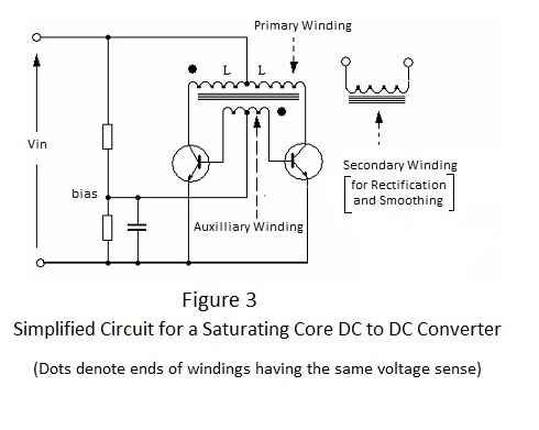
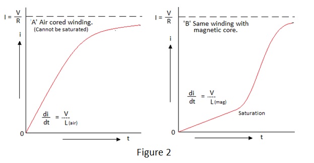
In the simplified circuit depicted in Figure 3, the primary inductors constitute a centre tapped winding with the tap connected to the primary power source Vin and the winding ends connected to transistor switches. Accepting that, at any instant, when one switch is on the other is off; the winding connected to the ‘ON’ switch will have Vin applied to it. The total primary winding constitutes an auto transformer and consequently the end connected to the ‘OFF’ switch must be at a potential of 2Vin; a factor to be taken into account when selecting the type of transistor to be used. A coupled winding, also centre tapped, is connected at the tap to a point which produces a low forward bias at the transistor base terminals connected to the ends of the winding. The turns on this auxiliary winding are such that each half generates a volt or so and the sense of its connection is such that the voltage generated enhances the forward bias for an ‘ON’ transistor switch and opposes the bias applied to its companion; holding the latter in the ’OFF’ state. From the instant a transistor is switched on, its collector current rises linearly until the onset of core saturation, as shown in Figure 2B. At the onset of saturation the current starts to rise steeply but the coupling between the primary winding and the auxiliary winding weakens due to the effective loss of a ferromagnetic core to concentrate the magnetic flux linking them. Thus the base drive voltage for the ‘ON’ transistor becomes insufficient to maintain its collector current –let alone increase it – and the reverse voltage at the base of the ‘OFF’ transistor becomes insufficient to prevent it from conducting. The action of falling conduction for one transistor and rising conduction for the other is cumulative; resulting in a reversal of the on/off status of the transistor switches each time saturation current is reached. Thus an alternating square wave voltage of amplitude 2Vin is applied to the primary winding. The half period of this waveform is the time for the current in each half primary to reach the level for core saturation and, as this period varies inversely with Vin, the running frequency is proportional to Vin.
The third winding shown in Figure 3 – the true secondary – generates the voltage required for rectification to the required dc. level, the number of turns being governed by the relationship between primary turns and primary voltage with an allowance for rectification losses.

This winding has work to do, i.e. it has not only to generate a voltage but it also has to supply current to a load. Now transformer theory decrees that, if the secondary of a transformer supplies current, an equivalent current – given by the product of the secondary current and the inverse of the turns ratio – must be drawn from the input supply by the primary winding and, by virtue of the fact that the drive waveform is a square wave, this current is of square wave form. Thus the current flowing in one half of the primary takes the form shown in Figure 4.       

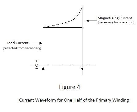
From Figure 4 it can be seen that the ramp of magnetising current, necessary to make the transformer work, rides on a much larger ‘block’ of load current. This is a necessary condition for efficiency, as the former plays no plays no part in the transfer of power from primary to secondary. The astute reader might ask why a high load current can flow in the primary winding when, as already has been discussed, it reaches saturation at a relatively small magnetising current. The answer to this is that the effect of load current in the secondary winding is to demagnetise the core and it is therefore necessary for the primary winding to draw the appropriate current to maintain magnetisation. Thus primary load Ampère-turns cancel secondary Ampère-turns such the net Ampère-turns applied to the core remains unchanged from that for the unloaded condition.
It has already been mentioned that the ‘spike’ of magnetising current impairs efficiency and makes for difficulty with regard to meeting electromagnetic  interference limits and the question might be asked “ Cannot switching be arranged to occur just prior to the onset of saturation?” assuming that it is not wished to operate at a significantly higher frequency. The answer to this is “Yes” and some possibilities are considered in the circuits depicted in Figures 5,6 and 7.  

Other push–pull Converter circuits                                                                                                                    

All of the following circuits are shown in their simplest form and for optimum performance additional components might be required. These additional components usually minimise the effects of the non-ideal performance of the transistor switches. Also the circuits do not address rectification, stabilisation and regulation and they show only a single secondary winding. There is no reason why the circuits are limited to the generation of a single voltage supply and further supplies can be provided by additional secondary windings. With regard to stabilisation and regulation, it is customary for the input voltage Vin. to be the output of a linear voltage regulator, particularly when a number of secondary supplies are required. This is quite satisfactory when the secondary loads are fixed because the converter source impedance is relatively low, but efficiency can be poor if the circuit is required to operate with a wide variation of the primary power source voltage; particularly when the latter is at the high end of its range. Secondary supplies can of course be regulated but this is obviously not cost effective when multiple supplies are required.                                                 

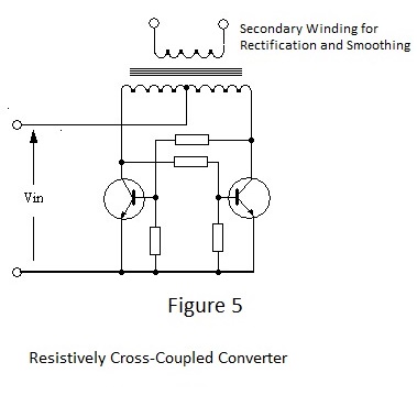
Figure 5 shows the simplest type of push-pull converter circuit. It has no auxiliary feedback winding to provide the appropriately sensed drive to the base terminals of the transistor switches, the base drive for an ‘ON’ switch being obtained by resistance coupling from 2Vin. potential at the collector of its ‘OFF’ counterpart. Pre-saturation switching can be effected by arranging this cross coupling to limit the base drive and consequently the available collector current of the switch transistors. This, however, is not really practical due to the wide variation of the HFE. parameter for transistors of a given type and restricting collector current to that required for operation obviates any capability for the supply of significant load current. Therefore the output impedance tends to be high and the running frequency to be load dependent if switching is not controlled by core saturation.

It must be concluded therefore that core saturation is still the dominant factor determining the switching periods for practical applications. Despite these shortcomings, this type of circuit has been used extensively because of its simplicity and avoidance of the need to take account of the sense of windings in its operation.

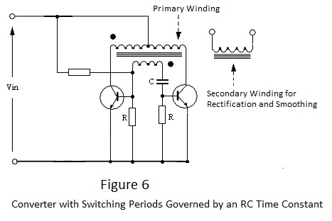
The circuit of Figure 6 imposes strict control of the switch ‘ON’ periods which can be set to preclude the magnetising current from reaching saturation. It employs an untapped and ‘floating’ feedback winding to generate the essential base drive current. However, in this case the winding is coupled to the transistor base terminals via series resistance and capacitance. The effect of this arrangement is to cause an initially high level of base drive current to taper off during the ‘ON’ period as the capacitor charges; the period being effectively controlled by the time constant produced by capacitor C and one or other of the two resistors R. The other resistor shown in the circuit, which is of much greater value than R, is necessary to ensure starting.
Correct sensing of the feedback winding relative to the primary is essential and the polarity of the voltage generated reverses for alternative half cycles of the switching waveform. Correctly used, the circuit operates free from the transient effects of core saturation and the effect of one aspect of imperfect transistor switching (delayed switch-off due to minority carrier storage) is reduced by the progressively falling base drive but correspondingly the output impedance is relatively high.

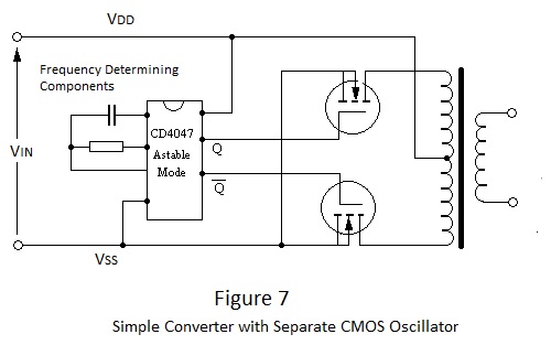
The circuit shown in Figure 7 is the author’s favourite type of push-pull converter as it overcomes most of the problems discussed or mentioned in the foregoing. It utilises MOSFET switches in lieu of bipolar transistors, a method which became practical for power converters with the advent of vertical gate technology. Mosfet switches have two distinct advantages over bipolar transistors: being majority carrier only devices, there is no problem of delayed switch-off and secondly they are voltage driven which obviates the need to supply significant current and consequently enables them to be driven efficiently by the Q and not Q outputs of a separate CMOS astable oscillator, as shown in Figure 7. There is of course no need for an auxiliary feedback winding and the component count is low.

Switched Mode Converters
In the foregoing discussion it has been stated that the current in the primary winding of a transformer necessarily comprises two separate components:  magnetising current to make it work and reflected load current from the secondary. It might therefore be surprising to find that in one type of converter circuit power transfer is achieved solely through magnetising current. Converters of this type are generically termed Switched Mode Converters.    
The term ‘switched mode converter’ came into vogue in the late seventies and the author personally considers it to be nonsensical – all the converters discussed so far operate by switching. Adoption of the generic term suggested the advent of a new operating principle but in reality converters operating by the storage and transformation of energy in a magnetic field have been around much longer than the push-pull variety; examples being vehicle ignition, television line deflection and what were known as ringing choke converters. A more apposite description might be choke or inductive storage converter. Switched mode converters are generally much more efficient than other types particularly in battery powered applications where the voltage of the primary power source is small or varies over a wide range. They are perhaps less suited than push-pull converters to applications where there is a wide variation of loading  as well as supply voltage but this is not usually a problem because supplies are normally designed for fixed loading.
Switched mode converters (smps.) are self-stabilising; the oscillatory control circuits operating within a servo loop to produce a stabilised output voltage, which is the main reason for their high efficiency. Their popularity has resulted in the availability of a wide range of integrated control circuits, which effectively require only consideration to be given to the design of an inductor for simple applications. However great attention must be paid to physical layout if the relatively high inductive currents involved are to be prevented from turning them into enthusiastic generators of electromagnetic radiation - somewhat paradoxically in view of high efficiency and the absence of core saturation. Another constraint is that the parameters input voltage, output voltage, load, frequency, inductance and peak current are uniquely interdependent such that, only by having some defined by specification and some defined by practical considerations, can others be fixed. A sort of chicken and egg situation as will emerge:
Operating Principles of Switched Mode Power Supplies.
The basic arrangement of a step-up voltage converter is shown in Figure 8.

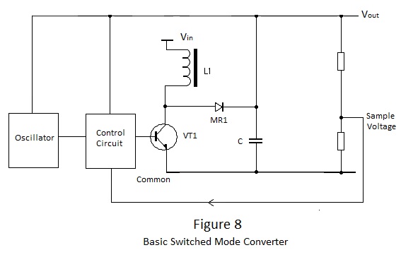
In this arrangement a variable voltage generated by L1, is added to the variable primary supply voltage Vin to provide a stable voltage Vout at a given power Pout. The arrangement shown in Figure 8 is not sacrosanct and other configurations are often employed, eg. the voltage generated by L1 may be subtracted from Vin to produce a step down converter or it may be referred to common to make it the actual output voltage. Also, using L1 as a primary, coupled windings may be added to produce additional supplies; their individual power outputs being included in the total Pout.
Smps. function by the storage of energy in a magnetic field and its subsequent recovery under desired voltage and current conditions. In the Figure 8 arrangement the switch (transistor VT1) is open and closed cyclically. During its closed period current through L1 increases linearly so that the energy stored per cycle is proportional to the square of the current reached and consequently the square of the closed period. The rate of change of current is determined by Vin/L and the period is terminated when the current reaches a predetermined level ( Imax) which is sufficient to satisfy the energy transfer requirement but is not so great as to overload the primary power source or to make its switching difficult. At Imax switch VT1 opens and the current falls at a rate determined by the output loading. By this means energy is transferred to the load with L1 acting as a generator of an emf. which is dependent upon the magnitude of the load – ‘highly confusing but hopefully it will become clearer as the discussion develops’. The efficiency of energy transfer is limited by the resistance of L1 and the individual efficiencies of the switch VT1 and the rectifier MR1 and, under ideal conditions, it can exceed 90%. It is obvious that the greater the power output requirement (Pout) the more of these cycles will be need in a given time, i.e. the running frequency (f) is proportional to Pout.
In a stabilised system Vout is smoothed by capacitor C1, sampled and fed back to control the oscillator running frequency, thereby regulating the rate of energy transfer to maintain Vout constant against variation of input voltage or load current Iout. The additional power needed to operate the control circuits must be low if high overall efficiency is the aim.
To satisfy the energy transfer requirement in the Figure 8 arrangement:-   

And, from the foregoing discussion the value of L1 depends on the value of Imax. Also, assuming that Pout is fixed, the running frequency must be maximum at Vin (min) and it cannot exceed the reciprocal of the transfer cycle period; upon which the value of L1 is also dependent. To extract ourselves from such a conundrum it is necessary to impose constraints:
Subject to the minimum defined in the expression, the value for I max is determined by practical constraints mentioned in the previous paragraph. The maximum running frequency is also decided by practical constraints – high frequency permits the use of low value and thus physically small reactive components (L1 and C1) whereas low frequency operation minimises radiative and core losses.
Having decided on Imax and fmax the value of L1 may be determined:-

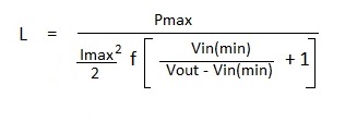
For the power levels and constraints involved  in a typical portable instrument application, the value of L1 for a 20kHz converter falls in the range 100μH to 200μH a value which could conveniently be wound air cored. However to minimise resistance and electromagnetic radiation the coil must be wound on a gapped magnetic core.
Recently switched mode converters have become common in mains powered equipment and plug- top power blocks. 

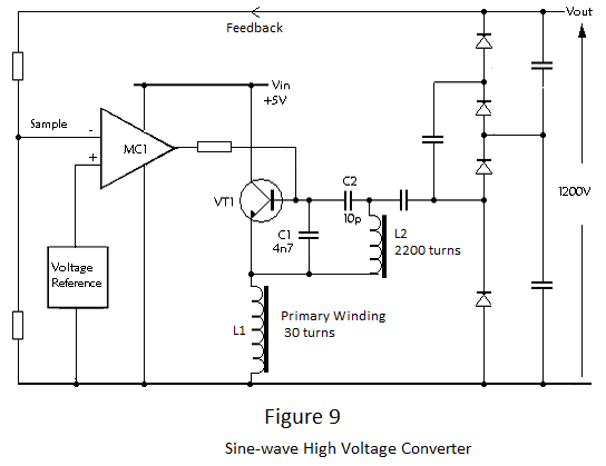
Sine –Wave Converters
Sine-wave converters have inherently poor rectification efficiency compared with converters which employ square waveforms, but for low power-high voltage supplies e.g. for photomultiplier tubes, they are ideal. Their main advantage is that the E field radiation from high voltage sinusoidal waveforms is much lower than would be the case with harmonic-rich square waves.
Referring to Figure 9, L1 and L2 comprise the primary and secondary respectively of a step-up transformer. L2 has seventy to eighty times as many turns as L1. L2 and C1 plus C2 form a tuned circuit which, by virtue of the fact that C1 is about 500 times greater than C2, has a resonant frequency determined by L2 and C2. These components, in conjunction with transistor VT1, are arranged to form what the author deems to be a transformer coupled Colpitts oscillator (others might call it something else). The oscillator operates in class C mode; the most efficient mode for sinusoidal oscillators. In this mode the transistor is biased such that it conducts only briefly during each cycle, with oscillation maintained by the flywheel action of the tuned circuit. With a supply of 5 Volts, the peak to peak voltage at the emitter of VT1 is about 8 volts and correspondingly the peak to peak voltage at the junction of L2 and C2 is about 600V. The voltage at the junction of L2 and C2 is coupled to a x 4 voltage multiplying rectifier to produce a dc potential of about 1200V. C2 and C1 form a capacitive potential divider to feed a small proportion of the voltage at the L2, C2 junction to the base of VT1 in order to sustain oscillation. The rectifier output voltage is sampled and fed back to an input of operational amplifier MC1; the output of which determines the base bias of VT1. MC1 compares the sample with a reference voltage to control and stabilise the rectified output.

Thank you for reading. Information given is free to use as you wish.