Back to Homepage & Index

This Page - Nuclear Pulse Amplification

All nuclear event detectors produce signals in the form of packets of charge.  For purely event detectors, e.g. Geiger-Muller counters, the charge produced is usually large enough to render its conversion to a form suitable for driving a counting circuit a simple matter but for spectrometric detectors, where the magnitude of the charge packet is proportional to the kinetic energy of the cause event, it is usually very small and requires careful amplification before application to amplitude selective counting circuits.  Detectors in this latter category include solid state and gas proportional detectors and, to a lesser extent, scintillation detectors.  It is amplification of signals from these devices which forms the subject of this note.

Analogue signal processing circuits normally work with a voltage signals with an amplitude range extending from zero to close to supply rail voltage.  It is therefore necessary to convert detector charge packets to voltage pulses and then to amplify these to a level suitable for processing. Because the signals at the early stages of conversion and amplification are very small, it is essential to minimise circuit noise if individual pulse amplitudes are to be resolved with precision.  The circuit which converts charge to voltage is known as a charge sensitive amplifier (CSA) or sometimes simply as a charge amplifier.


The essentials of a CSA are shown in Figure1 which depicts a low noise high input impedance operational amplifier with capacitive feedback with its input terminal connected to an ion chamber or similar source of charge. Without the justification of rigourous mathematical analysis of this circuit, the reader is asked to accept that, for a given detected event, capacitor C is charged to voltage V = -q/C where q is the charge produced by the detector.
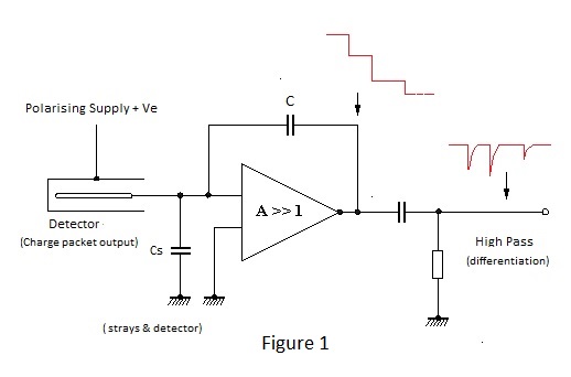
If, as invariably the case, the amplifiers open loop gain 'A' is much greater than unity, the voltage excursion at the input terminal is very small and a negligible proportion of charge q is diverted into charging of the stray capacitance Cs or to ground via any parallel leakage resistance.Because of the minute voltage movement at the input terminal, the amplifier is said to have a virtual ground input - a property common to most inverting operational amplifier circuits.
Thus the arrival of a detected positive charge at the input terminal causes a negative voltage step to occur at the output terminal of the amplifier and, unless the feedback capacitor C has a parallel resistance path to discharge it, this voltage remains static until another detected charge causes the output to step further; a series of detected events creating a staircase until the output of the amplifier is limited by the negative supply.
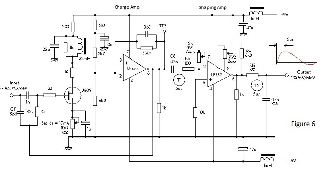
Voltage steps are of little use for signal processing and it is necessary to convert them to pulses by applying the amplifier output to a differentiating network (high pass filter) as is also shown in Figure 1. The rise time of the steps represent the charge collection time; a few nanoseconds for solid state and scintillation detectors and microseconds for gas ionisation detectors.
In order to obtain full signal transfer the differentiation time constant must exceed the charge collection time, however it must be small enough to prevent pulse pile-up at a maximum specified counting rate. Factors governing the choice of time constant are discussed later in this note.

It is obvious from the foregoing discussion that, unless the charge on capacitor C is leaked away by shunt resistance, an amplifier as depicted in Figure 1 would sooner or later become paralysed dependent upon the rate and magnitude of detected events. This resistance could be small enough to provide the differentiation mentioned in the preceding paragraph - and often is with scintillation detectors - but in the case of solid state or gas ionisation detectors, the reader is asked for the moment to accept that its value should be as high as possible and that differentiation should be applied later in the path of signal amplification.

To avoid paralysis in the amplifier depicted, the leakage reaistance R must be less than the negative supply voltage divided by the product of the mean detected charge and the maximum specified count rate. I.e. the maximum leakage current must exceed the current resulting from input charges arriving at the maximum specified detection rate.

For example assume a silicon alpha particle detector required to respond to 5MeV particles from activity producing up to 10,000 detections per second.  If the mean energy to release an ion pair in silicon is 3.5 eV, each alpha particle detected will release approximately 1.43 million electron charges or 0.228 pico Coulombs.  Thus, at 10,000 detected events per second, the effective signal current detector is 2.28 nA.  Assume also that the amplifier output can reach - 5V before being limited by proximity to the negative supply voltage.  The value of R must not exceed 5/22.8 x GΩ or approximately 2GΩ and a value of 1GΩ would probably be specified to be safe.
Consider now a value for C; if this is too great the voltage steps will be so small as to make voltage amplification difficult due to the noise introduced by the voltage amplifier and if it is too small, its true value will be indeterminate due to the influence of stray capacitance.  A value of 5 to 6pF is probably a fair compromise.

Assume C = 5pF, then the voltage step or pulse for our 5MeV event will be q/C = 0.228/5 = 46mV approximately.At first sight this appears to be a 'healthy' signal relative to amplifier noise - being of the same order as the input signals to audio amplifiers - and, in comparison with, for example, the signal from a gas proportional counter detecting 20keV X-ray photons, it is.  However, as will evolve in due course, parameters such as detector capacitance have a significant effect upon signal to noise ratio and amplifier noise can be a problem with solid state alpha detectors particularly when the requirement is to resolve particle energy with precision.

Let us now consider noise and how it may be minimised:- Noise is usually a problem in the first stage of a pulse amplifier, after which, with good design, the amplified signal is relatively large in comparison with noise introduced in successive stages.

There are three assessable sources of noise in amplifying devices and one which is which is less well understood.  The assessable sources are: a) Thermal noise produced by the input resistor, b) Shot noise produced by current flowing in the input circuit (including detector leakage) and c) Thermal noise in the controlled current path i.e. the channel of an fet, the cathode to anode of a thermionic valve or the emitter to collector of a bipolar transistor.  The fourth source, flicker or 1/f noise is usually only a problem with direct coupled amplifiers where it may be considered as a form of working point drift.

In this note discussion of these sources is limited to simplified statements of magnitude and effect. A detailed explanation of how they are derived is given in reference [1] which is recommended foundation reading for anyone interested in the application of electronics to nuclear physics.
A noise signal is alternating and random and thus it is not possible to define as a singular voltage or current.  It is therefore expressed in a manner which reflects the power it delivers to a load resistance; either as a mean squared voltage or current or, perhaps more aptly, the root of these values.

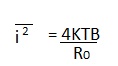
The mean squared noise voltage is equal to 4KTBR


                       Where   K is Boltzmann's constant
                                    T is Kelvin Temperature
                                    R is resistance (Ohms)
                                    B is the observed frequency band

Thus noise increases with temperature, resistance and the frequency band and, with regard to the latter, its value will always be the same for equal bands throughout the frequency spectrum; i.e. noise measured in the band 1000Hz to 1100Hz equals that in the band 100Hz to 200Hz.  Because of this uniform spectral density, thermal noise is referred to as white noise.

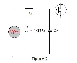
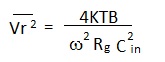
At first sight, the fact that noise increases with resistance does not square with the earlier proposition, that the value of the resistance providing a leakage path for the feedback capacitor C of a charge amplifier should be as large as practicable.  However the resistor may be considered as a noise voltage generator, of source impedance equal to its resistance, connected to the input terminal of the amplifier.  Therefore the actual noise voltage presented to the input is attenuated by capacitance between the input terminal and ground as shown in Figure 2.  This applies equally to resistors in the input signal path (as in the figure) or in the feedback path.  Note that this capacitance includes the capacitance of a detector connected to the input terminal in addition to the amplifier input capacitance.

Analysis of this simple circuit to determine the
mean squared noise voltage at the gate terminal
of the fet. yields the expression:-


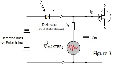
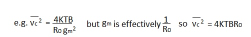
which demonstrates, perhaps somewhat surprisingly, that the effective noise signal reduces with increase of the value of resistance.

Consider now the second source of noise listed above - current in the input circuit as depicted in Figure 3.


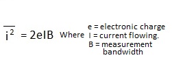
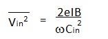
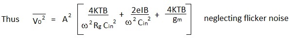
In the figure the value of Rg is large for the reason discussed above and consequently noise currents flow through almost entirely through Cin.  Shot noise apparently results from random fluctuations of the electron flow constituting a 'steady' current and consequently it is expressed in terms of noise current:-

Thermionic valves (now obsolete) were more satisfactory in this respect but paradoxically mosfets are much less so despite their low input currents compared with jugfets. To assess the effect of current noise upon the voltage driven   amplifier it is necessary to derive the mean squared noise voltage which it produces at the gate terminal:-


The expression for the third source of noise listed - thermal noise in the channel of our chosen fet input device - is similar to that for thermal noise current in a resistor only in this case the resistance Ro is, for those familiar with fet characteristics, essentially the reciprocal slope of the fet output characteristic below channel pinch-off.  For the purposes of noise analysis it is suffice to say that Ro is a resistor whose magnitude is controlled by the gate bias voltage.

As our analysis so far has been in terms of the mean squared noise voltage at the input terminal of the charge amplifier, it is necessary to divide the expression for noise current due to Ro :-

by the square of the mutual conductance of the fet.

i.e. the higher the mutual conductance the lower the effective thermal noise in the channel.

We have now considered the three most important noise voltage components at the input to the first stage of a charge amplifier and if this amplifier has a reasonable gain (> 10) noise produced by following stages will not have a marked effect upon the overall signal to noise ratio.  To find the mean squared noise output signal from the stage it is necessary to multiply the sum of the three components by A squared, where A is the stage gain. 

Taking the square root of the value of this expression, assuming its parameters can be quantified, gives us the rms. voltage of the random noise modulating the detector signal at same point in the amplifier circuit and we can determine the signal to noise ratio.  The modulation impairs resolution i.e. it produces uncertainty in the magnitude of a detected event, which would otherwise be  more precise, and steps can be taken to minimise its effect.  Referring once more to the expression, it appears at first sight that a high value for Cin is beneficial; this is not the case as too high a value for this parameter diminishes the loop gain of the charge amplifier in the frequency band of interest 'B', and reduces the signal to noise ratio.  Now 'B' appears in the numerator of each of the noise components and it is apparent that reducing it to a low value which does not markedly reduce the wanted signal, will optimise the signal to noise ratio.  Such bandwidth limitation can be applied to any point in the amplification chain and it is more practicable to limit the bandwidth of the voltage amplifier stage following the charge amplifier to than to limit the bandwidth of the charge amplifier itself.  There are a number of ways of limiting the band-with of nuclear pulse amplifiers, and tailoring the amplitude response within the band, to optimise the signal to noise ratio.  Reference [2] is recommended reading for anyone wishing to delve deep, but for the purpose of this note only the simplest and most 'cost effective' method is discussed.

We have already discussed the need to differentiate the output of the charge amplifier to form a pulse (Figure 1). and the chosen time constant Τ1 = CR determines the low frequency limit of the signal pass band.  If now a low pass or integrating time constant Τ2 is incorporated either within or following the voltage amplifier, this determines the upper limit of the band
as shown in Figure 4.


The shape of the amplified pulse is determined entirely by these time constants Τ2 defining its rise time and Τ1 its fall.  The closer the time constants are in value the narrower the pass band and, referring to Figure 4, it is easy to see that by bringing them closer together we can arrive at a minimum band for which full gain, and hence signal amplitude, can be achieved; anything closer resulting in signal attenuation and requiring additional amplification to achieve a target output. What if we take the limiting case Τ1 = Τ2 = t as depicted in figure 5?  In this circumstance the signal gain is reduced to 37% of the full signal and 2.7 times more gain would be required to achieve a given output signal than would be the case without bandwidth limitation

In fact the reduction in noise due to equal time constants outweighs the loss of gain and equal time constants are widely employed in nuclear pulse amplifiers. - Note that the time constants must not be iterative i.e. both cannot be incorporated in a single network; they must be separated by a buffer stage having high input impedance and low output impedance.  How is it arrived at?  It has already been mentioned that Τ1 must be greater than the detector charge collection time but must small enough to avoid the probability of significant pulse pile up at the highest expected detection rate and these limitations apply equally to a common time constant Τ.  It also must be realised that it controls the noise bandwidth B which features in all three components of noise mentioned above. In fact B = 0.33/Τ and thus a large value reduces the bandwidth and might be expected to reduce noise.  However things are not quite that simple: Note that the components for thermal noise due to the input resistor and for shot noise due to input current are frequency dependent i.e. ω appears in the denominator of the expressions defining their contributions to the overall noise.  The effect of this is actually to make the converse true i.e. these components are actually reduced by a small value for Τ (mathematical justification of this apparent paradox is given in reference [1]) whilst thermal noise in the channel is, as expected, reduced by a high value.  It can be seen therefore that the value chosen for t must be a compromise between requirement and device characteristics.  A value in the range 1 to 10µs is typically used for semiconductor detectors required to operate at detection rates up to around 20,000 events per second.

In the interest of minimising circuit complexity, shaping by equal time constants provides a good compromise for bandwidth limitation. Other shaping circuits produce better results at  cost. For example slightly better results might be obtained, at the expense of considerable added complexity, with what is known as Guassian shaping - due to the shape of pulse produced. Gaussian shaping involves a differentiating time constant followed by four integrating time constants. The latter are not iterative i.e. they separated by buffer amplifiers.

To see how the elements of nuclear pulse amplification which have been discussed are actually embodied in a working design, it is perhaps worthwhile to examine one.

Figure 6 is the circuit diagram of an amplifier which embodies the foregoing principles.  This circuit is designed to produce positive going pulses at its output, the amplitude of which are proportional to the energy of individual alpha particles impinging on a silicon detector; overall amplification being set to provide a scaling factor of 200mV/Mev.  The circuit has two sections: field effect transistor TR1 together with operational amplifier IC1 and associated components constitutes the charge amplifier and the circuit including operational amplifier IC2 provides voltage amplification to achieve the required scaling factor.

C11 is the feedback capacitor of the charge amplifier and its value results in negative voltage steps of approximately 6.7mV/MeV at TP3. 1GΩ resistor R22 shunts C11 necessary to prevent amplifier paralysis through charge accumulation; its value being as high as is practical to minimise the effect of the thermal noise which it generates.  Transistor TR1 is the input stage of the charge amplifier which is chosen and arranged to contribute the minimum of additional noise and to provide sufficient gain for its output signal to be large in comparison with noise introduced in following stages.  It is a field effect transistor with typically high mutual conductance (gm).  Thus contributions to noise resulting from the shot noise due to input current and thermal noise in the channel are kept small.  The value of gm which can be obtained is proportional to channel current and it is therefore usual for junction field effect transistors to be operated at zero gate to source voltage to maximise gm.  Unfortunately characteristics for individual field effect transistors of a given type vary widely; making it difficult to use them in this way in direct coupled amplifiers. In the amplifier depicted a compromise is arranged whereby TR1 is operated at the moderately high fixed current of 10mA in all units, by setting RV3 for zero volts at TP3.  Thus channel noise is kept to a reasonable, if not an optimal, low level.  Now the voltage gain for the fet. stage alone equals gm Rd (where Rd is the resistance in the drain circuit) and this needs to be at least 10 if the effect of noise from following stages is to be insignificant.

Thus if gm = 10mA/V, Rd needs to be 1kΩ or greater.  But a channel current of 10mA would result in a volt drop of 10V through 1kΩ which requires the supply voltage to be much higher than the 9 Volts used.  The drain load therefore comprises an inductance L1 shunted by a 1kΩ resistor.  Static volt drop due to the resistance of the inductor is small but at the frequencies intrinsic to the charge collection time its impedance is high and the drain load approaches 1kΩ for the pulse. Operational amplifier IC1 provides the essential loop gain for virtual ground input conditions.  It is arranged as a non-inverting amplifier with a gain of approximately 150. The overall loop gain is thus 2000 to 3000; a level which is adequate for the purpose whilst not prejudicing stability.  With regard to stability, the charge amplifier loop contains a number of leading and lagging poles and the input capacitance presented by the silicon detector is an essential component of the stability criteria. For stable operation the charge amplifier requires at least 150pF across its input terminals which is effected by the 500 to 600pF intrinsic capacitance of the detector.

The circuit including operational amplifier IC2 provides voltage gain to achieve the required scaling factor of 200mV/MeV and the bandwidth limitation necessary to 'optimise' the signal to noise ratio. C6 and R5 define the differentiation time constant and R13 and C8 the equal integration time constant of 5µs; giving the amplifier a - 3dB bandwidth of 66kHz.  Resistors R6, RV1, and R5 define a nominal voltage gain of 100, requiring IC2 to have a gain - bandwidth product of greater than 6.6MHz. but the overall gain is reduced to about 30 by the equal time constants shaping.
RV1 facilitates exact setting of the 200mV/MeV calibration and RV2 enables the output baseline to be set to zero by cancelling input offset potentials. 

References:

[1] 'Electronics for the Physicist   C F G Delany
Penguin Library of Physical Sciences - Penguin Books

[2] 'Electronics for Nuclear Particle Analysis' L J Herbst
Harwell Post Graduate Series Oxford University Press.

All content is free to use.