Back to Homepage & Index
This Page - Simple Applications of Operational Amplifiers
The Wien Bridge Circuit |
Despite the use of almost universal digital processing nowadays operational amplifiers still find application where it is necessary to interface with the real (analogue) world. For example it is often necessary to process the output of transducers to produce signals which are compatible with the input requirement for the adc. of a microprocessor chip. Also in simple stand-alone analogue applications a wide range of mathematical operations can be effected using a single fourteen pin dual-in-line package and some components.
Most manufacturers’ operational amplifier data sheets are supported by a plethora of examples of applications. Some simple but less common applications which have interested the author follow:
The Schematics and descriptions are free to use or reproduce.
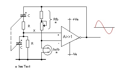
The Wien Bridge
(A circuit which forms the basis for a low distortion oscillator, a means of measuring total harmonic distortion and which spawned a mighty conglomerate).
 |
The frequency determining part of the Wien Bridge oscillator may be considered as a potential divider comprising a high pass filter in series with a low pass filter of equal time constant. |
This problem was addressed by two young MIT graduates Messrs. Hewlett and Packard back in the 1930s. They developed a way of making the gain determining negative feedback power sensitive and thereby to control amplitude and to minimise distortion. They started production and marketing of their sine wave signal generator from a garage and the rest is history. |
|
 |
|
The amplitude of the output is the voltage is that which causes the bulb resistance to be half that of Rfb and the power consequently delivered to the bulb is sufficient to make the filament glow. The value of Rfb may be adjusted over a limited range in order start oscillation and to set a defined output voltage. |
|
The Wien Bridge may also be employed to measure the total harmonic distortion in a waveform eg. the distortion in the output of an amplifier which is driven by a sinusoidal signal. Referring to the opening paragraph, the transmission of the frequency selective potential divider relative to its input may be expressed as 0.333 at 0 degrees for the fundamental frequency fo. For harmonics of the fundamental the transmission may be calculated as is tabulated:- |
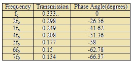 |
At first appraisal this table does not appear to show anything other than the transmission for harmonics is not dramatically less than that for the fundamental and that a lagging phase angle increases with frequency.
|
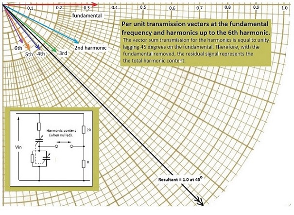 |
| The following figure shows how the Wien Bridge may be used to measure the percentage total harmonic distortion with the components to the right of the bridge amplifier constituting an ac. milivoltmeter circuit - the next topic for discussion |
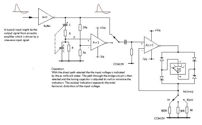 |
| An AC. Millivoltmeter Circuit. |
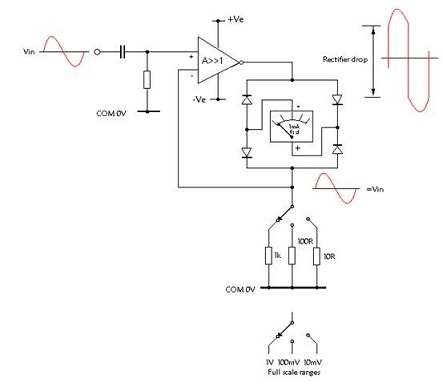 |
Measurement of small alternating voltages for display on a moving coil meter is subject to large errors due to rectification losses. Those who have AVO meters will be aware that a separate non linear voltage scales are provided for the lower AC ranges. This non-linearity is necessary to accommodate rectification volt drop which is minimised for the AVO by the use of a copper oxide bridge rectifier and a transformer which steps up low voltages before rectification. |
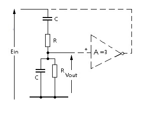
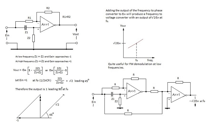
| The Frequency to Phase Circuit. |
The following diagram shows how an operational amplifier may be used to produce a constant voltage output signal; the phase angle of which (referred to the input signal) changes with frequency. |
 |
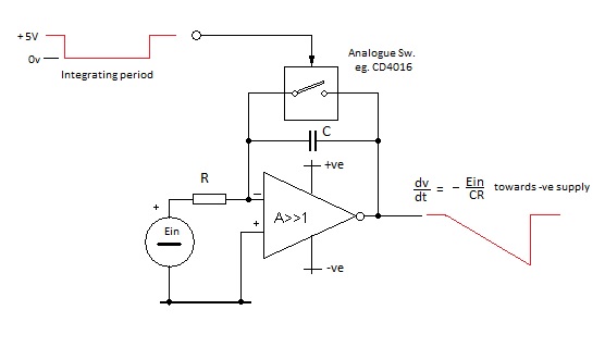
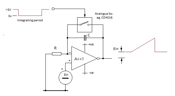
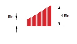
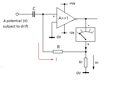
| The Rate of Change Circuit (Differentiator) | |
 |
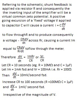 |
The purpose of this circuit is to produce an output which is proportional to the rate of change of the potential applied to the input terminal. It may be used to detect changes of a nominally fixed voltage irrespective of the magnitude of the voltage. An example of its application might be detection of the small step rise of the terminal voltage of a NiCad or NiMH battery as full charge is reached via constant current charging. This voltage step apparently occurs when the charging current ceases to do the useful work of chemical conversion and the battery becomes slightly resistive. |
|
| Variable Constant Current Generator | |
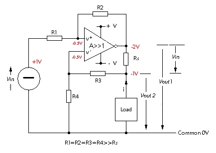 |
This circuit causes a high source impedance current which is proportional to the input voltage to flow in a load. Typical direct current applications might be battery charging or electro-plating and pulse applications might simulate devices which produce charge signals such as nuclear detectors - requiring only a voltage pulse input which mimics the profile of a charge pulse. |
| At first appraisal the circuit would be expected to have doubtful stability because both positive and negative feedback is applied. However stability is assured because the negative feedback exceeds the positive feedback provided that the equal value resistors R1, R2, R3 and R4 are of close tolerance. Also the value of these resistors must be much greater than the current defining resistor Rs; the circuit being best suited to operational amplifiers with fet. input transistors. | ||||||||
Referring to the circuit annotations; the circuit causes a current (Vout1-Vout2)/Rs to flow through the load circuit by virtue of the fact that V+ must be essentially equal to V- due to the high open-loop gain of the amplifier. V- can only equal V+ if there is a voltage (Vout1 – Vout2) across Rs and consequently For direct current applications it is possible to use the circuit in a non inverting mode with Vin applied between common and the end of R4 and with the input end of R1 connected to common. In this case it is necessary to introduce a dominant lag in the amplifier frequency response in order to avoid oscillation. This is achieved by connecting a suitable capacitor in parallel with R2. |
||||||||
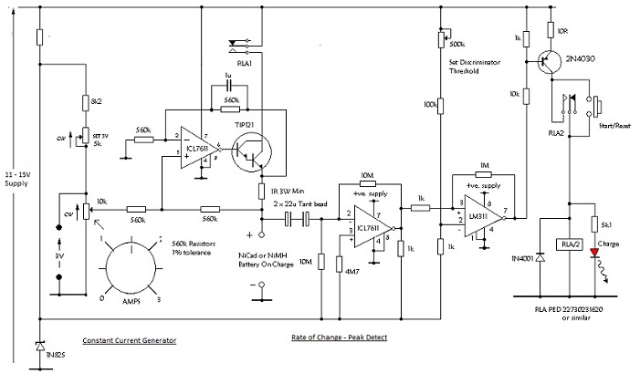
| An Example of the Application of the Preceding Two Circuits to NiCad/NiMH Battery Charging | ||||||||
| The following circuit is an example of how the above circuits might be incorporated in a practical charger for an 8 cell NiCad/NiMH battery with presetable charging current between 0 and 3 Amps. | ||||||||
|