This Page - Electrometer Amplifiers (for sub-picoamp currents)
Primary ionisation chambers, as described in Page 4 of this site, produce currents in a range from femtoamps to nanoamps (10 exp -15 to 10 exp -9) or wider. Special electrometer amplifiers are necessary to amplify such minute currents to levels compatible with normal electronic processing.
These amplifiers are often required to respond to a number of decades of input current either linearly (with manually or automatically switched ranges) - or logrithmically such that a wide range of input current can be displayed by an appropriately scaled analogue meter. Both types are discussed in the following:
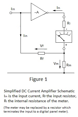
Figure1 shows a schematic for a direct coupled current measuring amplifier. The current flowing through the milliammeter, Im, is essentially equal to :- -IinRf/Rm [1]
provided that no current is diverted into, or fed from,
the amplifier input terminal and the loop gain:-
ARm/(Rm + Ri) is much greater than unity.
The amplifier must thus have very high input resistance, its voltage gain must be large and Rm must not be much less than Ri. From expression [1] it can be seen that Im is directly proportional to Iin and is equal to Iin multiplied by the factor -Rf/Rm -the current gain of the amplifier. It can also be seen from [1] that Im is independent of the resistance of the milliammeter and within reason any milliammeter may be used to indicate the magnitude of the input current.
The range voltage Vm is given by ImRm and inserting this into [1] gives Vm = -IinRf.
Therefore Vm is equal to, but opposite in polarity to, Vf the volt drop across Rf due to Iin. Of course Vf and Vm differ by the voltage needed to drive the amplifier, Vf/Loop gain, but if the loop gain is very high the drive voltage will be virtually zero.
As wii emerge in due course, this virtual-earth input is an essential requirement for current-measuring electrometers.
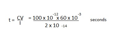
Consider the most sensitive range 20fA f.s.d. and assume that this is to be displayed by a 1mA f.s.d. meter.
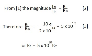
Thus it would appear that any combination of resistors having this relationship could be employed to achieve the desired result. However account must be taken of amplifier shortcomings - All direct coupled amplifiers are subject to drift , both as a random function of time or as the result of temperature change.
Fortunately, time dependent drift is relatively small in solid-state amplifiers but the effects of temperature have considerable bearing upon the choice of Vm.
In common with most solid-state direct-coupled amplifiers the electrometer amplifier is of the balanced differential type, having one input terminal driven by the input signal and the other held at an equal reference potential.
This of course minimises the direct effects of temperature and supply voltage change by rendering them common-mode and the degree of temperature dependence depends upon the matching of temperature coefficients of components of the balanced input stage.
All practical direct -coupled electrometer circuits will be subject to a degree of temperature dependence.
Unfortunately, due to the need for very low input leakage, it is essential to to use mosfet. transistors in the input stage of an electrometer amplifier; devices which can normally be matched to within 100 μV/degree in monolithic pairs.
Consequently, the virtual-earth driving point can drift by up to 2mV for a 20 degree temperature change. This effect, together with other sources of drift may be represented by an additional voltage generator as shown in Figure 2.
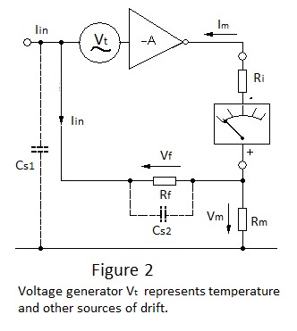
As Vt is within the feedback loop it must be small in comparison with Vm (-Vf) if the dominant temperature-dependent drift is not to be a nuisance. However the choice of Vm is constrained by the maximum practical value for the feedback resistor Rf and its relationship to Rm as defined in expression [3] above.
High value resistors are available in values up to 100TΩ
(10 exp14 Ω) but about 3TΩ is about the maximum value with 1% selection tolerance and stability in respect of temperature, voltage coefficient and ageing. This constraint defines Vm as 60mV for the 20fA f.s.d. range. For the higher ranges of input current it is possible to reduce Rf or to increase Rm and consequently Vm.
Of these options, the former gives the benefit of reduced response time -as is discussed later- and the latter is less costly because fewer expensive high value resistors are are required to accommodate the projected ten ranges of measurement. The latter also simplifies the range switch at the input to the amplifier with a consequent reduction in piezo electrically generated charge overloads during during range selection. In fact the range 20fA to 0.6nA can be conveniently covered by two values for Rf (3TΩ and 10GΩ) inconjuction with seven values for Rm.
Response Time.
Also shown in Figure 2 are stray capacitances Cs1 and Cs2 which can influence the response time of the electrometer amplifier. Cs1 represents the input capacitance made up by the capacitance of the signal source - ionisation chamber etc. - and the gate capacitance of the input mosfet. The magnitude of Cs1 might be as high as 100pF and by virtue of its position it must be charged by the input current before the electrometer can achieve a correct indication. Taking account of the fact that Vm is 60mV for the 20fA range, it is worthwhile to examine the the time required for the input current to charge 100pF to 60mV.
Therefore, without virtual-earth operation, f.s.d. would be reached after five minutes.
However for the most critiacal 20fA range, the loop gain ARm/(Rm + Ri) for the projected design is likely to exceed 40,000 if a typical operational amplifier is included in the loop and thus Cs1 will be charged to
60/40,000mV i.e. 1.5μV. This requires approximately 8ms and Cs1 is not significant with respect to its effect on response time.
Cs2 represents the stray capacitance across the high-value resistor and, until it is charged by the input current, the full range voltage cannot be developed across Rf. Cs2 and Rf thus produce a lagging response with a settling time constant T = Cs2Rf seconds and the indication may be considered to have settled after 3T. Cs2 is typically about 2.5pF and thus the settling time will be approximately 7.5 seconds for ranges employing a 3TΩ resistor. For these current ranges the output of the amplifier will reach 95% of its final value approximately 22 seconds after a step increase of input current. For ranges employing a 10GΩ resistor the response is much more rapid and it is sometimes desireable to create a similar response time by shunting the resistor with a low leakage polystyrene capacitor.
Input circuit.
As mentioned previously, a mosfet input stage is essential to prevent signal current from being diverted into the input terminal of the amplifier and to prevent it from being augmented by current from within the amplifier.
Mosfets are highly susceptible to breakdown of their gate insulation, due either to voltage transients or static discharges received through handling. Breakdown due to voltage transients is a problem with instuments employing ionisation chambers (see Page 4), since these often require polarising potentials of several hundred volts It is therefore advisable to protect the input gate with devices which break down or avalanche non-destructively at a voltage lower than that which would cause destructive breakdown of the gate insulation, and for less stringent applications Zener or avalanche diodes may be used for this purpose. However for electrometers the conductance of normal Zener diodes is likely to be unacceptable and special low leakage "picoamp" diodes are used. The simplified input stage of a typical electrometer is shown in Figure 3.
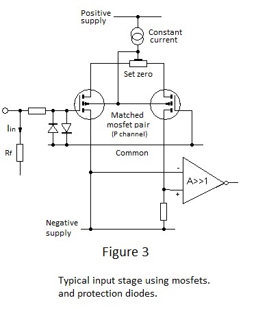
The gate-protection diodes are connected between the vulnerable input gate and the common 0V. In view of the requirement for negligible leakage, it might appear odd that the diodes are connected in parallel and thus apparently short circuit the input terminal to common.
However picoamp diodes are of very small area and are characterised by very low reverse leakage in comparison with ordinary signal diodes. This, in conjunction with virtual earth operation, ensures that leakage to common 0V is very small in comparison with the input current for the most sensitive range, provided of course that there is negligible voltage offset at the input terminal. However the diode leakage doubles for approximately every 7 degree rise in temperature and consequently a 20 degree rise might result in an eight-fold increase. With the input terminal at 0V the magnitude of the increased conductance is not excessive but, as discussed in connection with the choise of range voltage Vm for the most sensitive range, it can be accompanied by a voltage offset of 2mV.
Taken together, these effects of increased temperature can result in unacceptable offset current and it is therefore necessary to make provision for precise adjustment of the 'Set Zero' control to minimise the voltage offset, particularly at high ambient temperature.
The Set Zero control shown in Figure 3 compensates for differencesbetween the gate to source voltages for the mosfet. pair when Im=0: it is adjusted in a 'Set Zero' position of the range-selection switch, which short-circuits the high value resistor Rf and selects a lower value Vm. The control is normally a ten-turn potentiometer which, in conjunction with a Vm of the order of 10mV fsd., permits the offset voltage to be easily maintained within +/- 100μV of 0V.
In view of the fact that leakage through the protection diodes is rendered insignificant by vitual earth operation, why is it not practical to use bipolar or junction-gate field effect transistors (jugfets.) in the input stage? The answer to this question is that the internal leakage current, i.e.current to and from the input terminal from the other electrodes is too great in these devices.
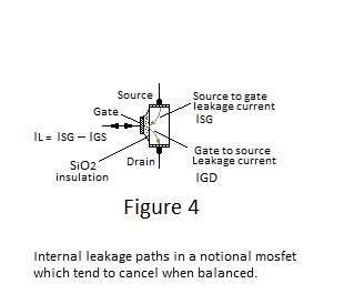
In mosfets. the internal leakage is minimised by the gate insulation to a level many orders below the base current for a bipolar transistor and several orders below the leakage across the reverse biased gate junction of a typical jugfet. Even with mosfets. it is advantageous to minimise offset current by arranging equal gate-to-source and gate-to-drain operating voltages, under which condition the internal leakage currents in a notional transistor - as depicted in Figure 4 - tend to cancel. This balanced operation also cancels external inter-electrode currents due to leakage across the header, which can be minimised by installing the electrometer amplifier within a desiccated sealed compartment.
Once freely available, matched dual mofets. are now difficult to obtain; semiconductor manufacturers presumably finding the market for them too small. However integrated circuit electrometer amplifiers have been developed for smoke detectors and these can be used for more general application with careful design. For some reason some of the ad hoc. smoke detector amplifiers operate without virtual earth input and package leakage is minimised by bootstrapped guard pins either side of the input pin.
Logarithmic Electrometers
For some applications of electrometer amplifiers, a single-range logarithmic display is a convenient way of presenting measured data, particularly for process monitoring applications where a wide dynamic range may be displayed on a suitably scaled strip chart or meter for 'at a glance' interpretation. Freedom from the disturbances attendant upon range switching operations are an added advantage of this mode of operation.
It is well known that, if the feedback resistor of the conventional operational amplifier circuit is replaced by a junction diode, the amplifier output is a function of the logarithm of the input signal and it might be of interest to see how this principle is applied to a logarithmic version of the projected electrometer amplifier.
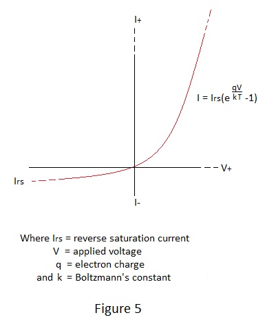
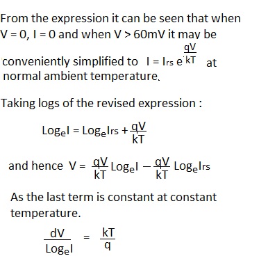
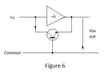
In this arrangement Iin = Ic which closely approximates to Ie if HFE is high and constant. External leakage is minimised by the use of a transistor of small area and, for this reason, the transistor is often reversed to make its emitter the input terminal. It being the smaller electrode in an epitaxial transistor.
The lower level of input current to which the logarithmic relationship extends is governed by external by external leakage and by recombination current within the transistor, and few discrete devices are suitable for use down to femtoamp levels.
However some of the very small geometries used in l.s.i. microcircuits are well suited to the application.
The upper limit of the input current range is determined by ohmic resistance within the transistor but this only becomes significant at input current levels well above the projected maximum, even for devices of such small area.
This would be insufficient to drive, for example, a simple strip-chart recorder efficiently and further amplification is desireable. A following linear scaling-amplifier also facilitates back-biasing to 'zero' the recorder indication for the lowest current to be measured and the means to effect compensation for the temperature dependence of the feedback element.
If Vbe is plotted against log10Iin, the curve produced will of course be a straight line over the range of input current for which the logarithmic relationship holds; the slope of the line being 2.3026kT/q volts per decade,as derived previously. Thus the slope of the line varies directly in accordance with absolute temperature. To compensate for this temperature dependence,the gain of the scaling amplifier is made to vary inversely with absolute temperature. by means of temperature dependent feedback. A simple network, which embodies a n.t.c. thermistor, as shown in Figure 7, can be arranged to provide almost ideal compensation.
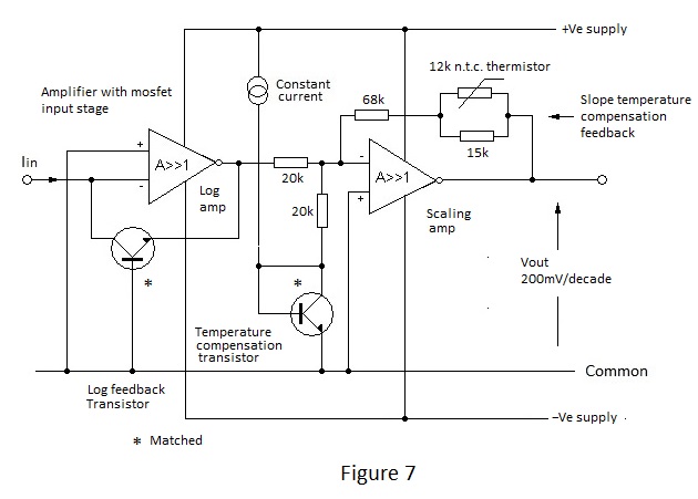
Having compensated for slope dependence upon temperature, the straight-line Vout versus LogIin response will be observed to be displaced by change of temperature - i.e. there is temperature-dependent 'scale-zero' drift. The magnitude of this drift cannot be directly derived from the simple diode equation, because it is the result of the temperature dependence of Irs, but it is the familiar -1.5 to -2.5mV per degree dependence exhibited by forward-biased semiconductor junctions. This can be compensated by deriving the reference bias for the scaling amplifier via a transistor identical to and close to the log.feedback transistor, i.e. these transistors should be a matched monolithic pair.
Compensation for the temperature dependence of 'scale-zero' is shown in Figure 7.
The foregoing is free to use. Thank you for reading.
Addendum
In a practical circuit the electometer input needs to be connected to the signal source e.g an Ion chamber.
For this purpose a stand-off insulator teminal is often convenient. Prima facie a PTFE barb inaulator would appear to be the ideal solution to this requirement but in fact PTFE is probably about the the worst material which can be used and glass or ceramic stand-off insulators are recommended.
The reason for this is that PTFE undergoes a 'first order' specific volume transition between 19 and 21 degrees centigrade. For a constrained assembly like a barb insulator the 'immense' Piezoelectric charge produced is sufficient to damage a sensitive electrometer or at least paralyse it temporarily
The author happened upon this phenmenon many years ago when the property was not widely acknowledged
but nowadays it is recorded in the Dupont specific literature on PTFE.