Back to Homepage & Index
This Page - A simple Signal Source for testing Crystal Receivers
Last year my old friend Dave Warren asked me for some tips with respect to making a crystal set like one he had made in his youth. From my perspective it would be a case of some ‘know what’ as opposed to ‘know how’ because I have never made a decent crystal set.
It rapidly became apparent that one stood a better chance of making a successful crystal receiver in the late 1920s than now; firstly because of the dearth of long and medium wave transmissions and secondly the lack of suitable components like tuning capacitors, 'cats whiskers' and earphones.
However for the time being the BBC’s ‘gold standard’ of Radio 4 Long Wave and a few MW stations are still on air so it is still worth the effort.
Somehow the receipt of intelligence using only the energy contained in a wave travelling through the ‘luminescent aether’ is appealing.
Probably the best time to build a crystal set was in the 1950s. The ferrite rod had just appeared to facilitate the winding of simple and neat coils, excellent air dielectric tuning capacitors were available (often with 3:1 reduction gearing in the end of a ¼” diameter shaft) as were point contact Germanium detector diodes; the latter being a spin off from microwave mixer diodes used in WW II.
Nowadays we are faced with miniature plastic dielectric tuning capacitors which tend to be lossy and are inconvenient to use and diodes which are as not as good as might be thought.
With regard to the latter forward conductance is the crucial parameter: Silicon junction rectifier diodes (e.g. IN4148, 1N916 etc.) are useless and Schottky versions (1N5711 etc.) are little better.
What are required are Germanium diodes, preferably point contact, but junction versions are satisfactory for h.f. detection.
These conclusions result from the search for a diode to detect microwaves by the author and friend Terry Tippett, with whom is shared a website (norcim-rc.club/index.htm) primarily concerned with the radio control of models. Details of diode tests are given in pages of the Norcim site and Page 16 of this site.
Dave Warren’s LW/MW crystal set would be an opportunity to gather further information on the relative effectiveness of various diodes partiularly because Germanium diodes are getting difficult to source; with many sold as such being in fact Silicon Schottky diodes.
The upshot of this preamble was that Dave was able to build a satisfactory crystal set and provide comparisons of the relative efficacy of various detector diodes.
He was also keen to see if the set could be improved; an aim hampered by the lack of basic test equipment other than a DMM.
It was therefore decided that a simple amplitude modulated signal source would be useful; the design of which is the subject of this page.
What would be required would be a simple r.f oscillator capable of producing low level Long Wave and Medium Wave signals either continuous or audio modulated to a depth of approximately 30%.
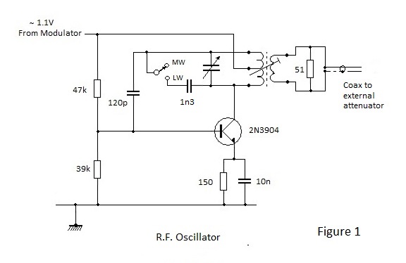
The Oscillator
The schematic for the r.f. oscillator section is shown in Figure1. The oscillator is intended to produce a low level signal which covers most of the medium wave frequency range together with a signal of limited frequency range which 'brackets' the BBC Radio 4 transmission on 198kHz.
The circuit comprises a single transisitor tuned collector oscillator powered by about 1.1 volts supplied by from the audio modulator circuit
The oscillator circuit employs a modified 455kH Toko I.F transformer which is tuned over part of the medium wave by a variable capacitor souced from an AM/FM radio and which replaces the inbuilt fixed capacitor of the transformer. The latter can be removed by dismantling and desoldering it but, as it is a tubular ceramic device, it is easier to destroy it by poking a sharp instrument into the receptacle in the bottom of the transformer where it is located. Long wave operation is effected by switching in padding capacitance to give a tunable frequency range of 190kHz to 202kHz.
The output signal is taken from the transformer secondary winding which is loaded by 50Ω and fed to a coaxial cable for further attenuation external to the metal case of the signal souce.
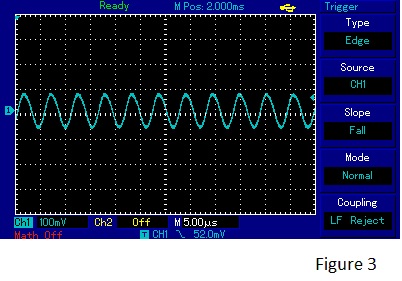
As can be seen it is an undistorted sine wave of around 140mV pk.to pk. The MW waveform exhibits a small amount of even harmonic distortion which is all to the good because the tuned frequency range doesn't fully cover the medium waveband. Higher frequencies in the band can thus be attained as second harmonics albeit with much reduced output.
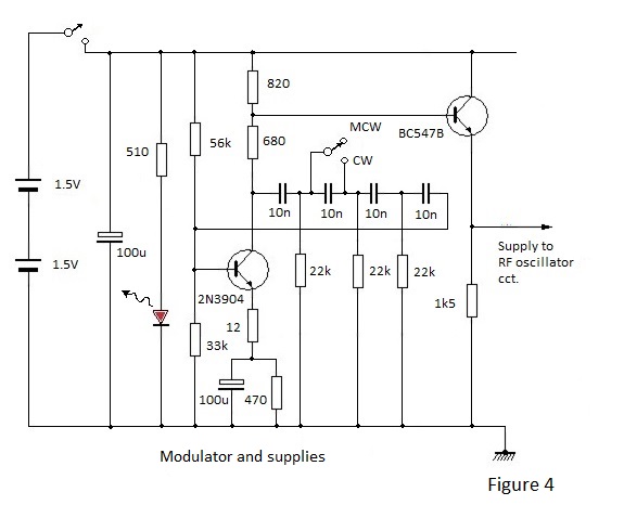
The Modulator
The schematic for the modulator is shown in Figure 4. It is based upon a four stage phase shift oscillator running at around 330Hz. Four stages are used because less signal is lost by four stages of 45 degrees of phase shift than is lost by the more conventional three stages of 60 degrees and consequently less gain is required for oscillation. Use of this is made for CW operation where the oscillator is stopped by effectively removing a stage of phase shift by shorting circuiting a stage with a switch.
Oscillations at the collector of the 2N3904 transistor are fed to an emitter follower via a potential divider. The standing output of the emitter follower provides a nominal 1.1V supply for the r.f. oscillator. Thus, when MCW is selected, this supply is varied at 330Hz and consequently it modulates the oscillator output
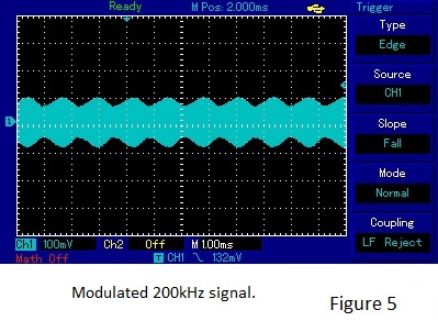
The LW modulated output from the Signal Source is shown in Figure 5 which demonstrates a modulation depth of around 30%. Because of the harmonic content of the medium waveband signal, the modulation envelope is less symmetrical but this is of little consequence.
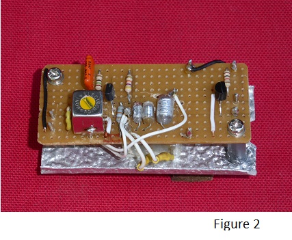
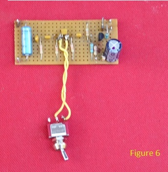
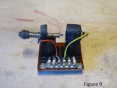
The components of the four stage phase shift oscillator are mounted on a strip board which is similar in size to that used for the R.F. Oscillator circuit. The arrangement is shown in Figure 6. together with the switch which short circuits a capacitor for CW operation.
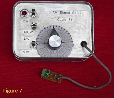
Also shown in figure 7 is the termination arrangement which facilitates further signal attenuation and the attachment of radiating wires or loops.
Page under construction with the possibility of reports of application of the Signal Souce dubbed Covid 19 in reflection of it being a 'lock down' project.
Addendum:
'The Cats Whisker'
Few, if any, listeners still used crystal sets when a was a boy but some must have retained examples as curiousities and my first encounter with one fired my interest. Here was a magical device with which one could receive radio broadcasts via 'electricity in the air' without need of mains electricity, dry batteries or accumulators. I imagine that the example which I tried was blessed with a long aerial and sensitive headphones because it was possible to tune to, and to hear clearly, a number of long and medium wave stations.
The quality of reception appeared to be dependent upon one's 'touch' with respect to the the adjustment of the mysterious cats whisker rectifying detector which was in effect an unsealed point contact Galena (Lead Sulphide) diode.
My recent attempts to produce a crystal set indicated that the benefits of subsequent developments in semiconductor technology have not necessarily been beneficial in this respect and that efficient direct demodulation of a weak radio signal is crucially dependent upon the forward conductivity of the rectifying diode. Consequently current silicon diodes of all types including Schottky diodes are of little use and that the only serious candidate for replacement of the Galena diode was the, now obsolete, point contact Germanium diode. Germanium signal diodes are available from on-line sellers but, 'caveat emptor', many which are sold as such are silicon Schottky diodes.
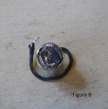
To satisfy myself that there is nothing magical about the Galena diode I decided to make a 'cats whisker' detector for comparision with its Germanium counterpart. Galena crystals are readily available from on-line sellers and a main problem was how to make good ohmic contact with a 'craggy' lump of crystal. Research indicated that the recommended method for mounting Galena Crystals was to partially immerse them in Wood's metal (a multiple metal eutectic alloy having a much lower melting point than 60-40 tin/lead solder) and consequently this was the method adopted. With the object of providing a degree of axial advance or retard of the crystal face, I decided to mount the crystal in the MES. cap of a defunct flashlight bulb as shown in Figure 8.
A basic circuit arrangement for plotting forward conduction characteristic of the Galena diode is shown in Figure 10.
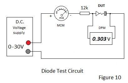
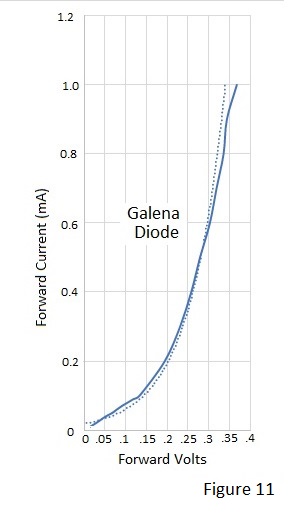
Figure 11 shows the result of preliminary measurement of the forward conduction characteristic of the Galena diode.
Matched to the characteristic is an exponential trend line which demonstrates that the conduction is much as would be expected for a classic semiconductor. With a less 'hit or miss' method of detecting a rectifying contact than pure chance, the characteristic might be determined with sufficient precision to afford direct comparison with a good Germanium point contact diode. E.g 1N34A.
Even when 're-inventing the wheel', it is pretty certain that someone else is doing the same thing and making a better fist of it.
Researching the subject, Terry happened upon an excellent 'youtube' video which provides the solution to the problem of locating a good contact (https://www.youtube.com/watch?v=2yzr4kx8SJ4). In this video an engineer uses demodulation of an amplitude modulated radio frequency signal and an oscilloscope to identify'sweet spots' on the surface of a Galena crystal and I decided to adopt the method in order to establish a good connection for plotting an I vs.V characteristic.
What I found using this method was interesting:- Firstly, with my ' whisker assembly' and contrary to what I had read on the subject, making a rectifying contact is not difficult and secondly that a really good contact can readily identified by the amplitude and purity of the demodulated signal. Perhaps the use of nichrome for the whisker might have something to do with this? (My inital tests using a Beryillium Copper
whisker were not encouraging).
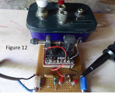
The rig for pre-checking contact quality prior to plotting an I vs.V charteristic is shown in Figure 12 opposite.
The green/blue box being a coax lead
commoning facility for the signal source
and demodulator. Two red spring terminal posts
facilitate substitution of a reference diode
with the cats whisker disconnected.
The input is a 2MHz waveform with
about 30% 400Hz sinewave amplitude
modulation. However the rf. waveform
is not sinusoidal but rich in second
harmonic content to double
the effective frequency range.
This does not display well on an 'orrible
digital scope but the demodulated
output is shown is shown in Figure 13
below:-
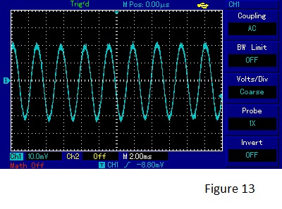
Attempts to plot a more precise characteristic than that shown in Figure 11 did not result in significant improvement. The Figure 11 plot was made using three separate moving coil meters for the current measurement and it was thought that the unavoidable physical disturbance might have had a detrimental effect on the crystal contact. However the result of a repeat test, using a digital current meter to cover the range and provide precise indications, was not signifiantly different.
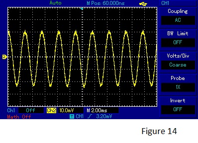
Having established that the rectifying contact was essentially stable, the demodulated carrier
arrangement was allowed to run continuously for about 24 hours before repeating the measurment; the result of which is shown in Figure 14 below:-
The conductivity of various Germanium diodes was checked using a DMM. for an example or type exhibiting the lowest forward voltage drop at the test current. The lowest voltage drop of 270mV was exhibited by
a DO7 packaged diode marked 0A90 and which was therefore selected for direct comparison with the Galena diode. The next best contender at 281mV was astonishingly a BAT85 Silicon Shchottky diode, closely followed at 283mV by a D035 packaged IN34A Germanium point contact diode recently purchased from 'Loudatronics'
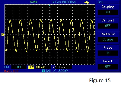
Comparing the peak to peak amplidudes of the waveforms, there appears to be nothing to choose between the response of the Galena 'Cats Whisker' diode and a manufactured Germanium counterpart.
However, looking carefully, it is apparent that Figure14 depicts a 'pretty good' 400Hz. sinewave whereas a hint of harmonic distortion is apparent in the Figure 15 waveform.
Perhaps after all there is some magic in the Cat's Whiskers after all!
Iron Pyrites was an alternative crystalline material used for Cat's Whisker detectors and it was decided to compare its properties with those of the better known Galena diode.
Like galena, single cubic crystals are found in amorphous pieces of shiny rock (Fool's Gold). They tend to be smaller than their lead based counterparts and more difficult to separate from the bedrock. In fact the firework display occasioned by breaking the rock with a hammer to remove crystals warrants the name Pyrites.
Having obtained a couple of small crystals, the better of the two was mounted in Wood's metal in an MES bulb shank in a similar manner to to the galena crystal. However the small size necessitated restriction of the lateral range for contact by means of an insulating ring as shown in the photograph Figure 16.
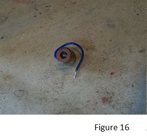
In the photograph it is just possible to see a face of the crystal through the aperture afforded by the red fibre washer.
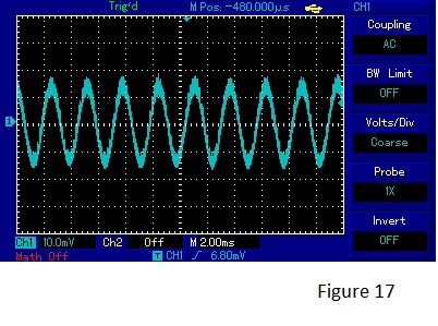
The 'stable' resonse of this detector to the 2MHz modulated carrier is shown in Figure 17 opposite.
From Figure 17 it is concluded that the output of the pyrites detector is around 75% of that of the galena detector, also more noise content is apparent in the waveform irrespective of the reduced amplitude.
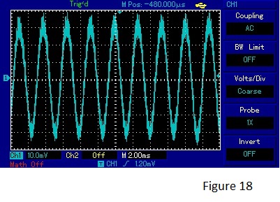
However very occasionally the output appeared to double for no apparent reason. This increase was uncharacteristic of the improvement related to the achievement of an improved rectifying contact. In fact
is was more what might be expected if amplification was involved. This possibilty was discounted until it was recalled that, unlike junction transistors, early point contact germanium transistors exhibted a small degree of current gain when operated in common base mode. A property mentioned in the index page to this site.
A document search revealed that the pyryites diode can operate in a similar manner to a tunnel diode:-
http://www.sparkbangbuzz.com/els/iposc-el.htm
In this reference an engineer demonstrates that not only can the pyrites diode exhibit negative resistance, but he employs the property in a practical application.
The 'amplified' response obtained for the subject of the current investigation is shown in Figure 18 opposite.
With the employment several instruments to obtain the characteristic for the Galena ‘cat’s whisker’ detector it was difficult to avoid disturbance of the surface contact. The solution to this difficulty would be a ‘snapshot’ oscilloscope trace. Thus an ad. hoc. curve tracer circuit was constructed for this purpose. In fact, the curve tracer was constructed originally for the purpose of acquiring the tunnel diode characteristic shown in Figure 13 of page 19 of this site.
To obtain a diode characteristic it is better to employ voltage drive to the anode and to measure the current passing concomitantly through the cathode return. The alternative of current drive with voltage measurement is not applicable to devices which exhibit negative resistance in a region of the characteristic.
The applied forward voltage having, by definition, low source resistance must not exceed a level which would result in destructive current flow. Consequently, it was decided that the applied forward voltage should be limited to a maximum of approximately 0.6V and, given that ability to withstand high reverse voltage is not applicable to a signal detection diode, reverse bias was limited to approximately 2V. Thus, for curve tracing the applied voltage signal is a linear ramp, rising from –2V to +0.6V.
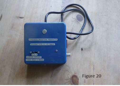
It operates from +/- 5V dc. supplies and it is housed in the unit shown in Figure 20 with a mains power unit, making a self-contained test generator.
The peak voltage is dependent upon circuit component tolerances.
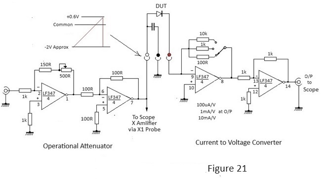
Consequently, an adjustable operational ‘attenuator and buffer’ circuit facilitates adjustment of the applied peak voltage. This is housed separately in a 2oz. tobacco tin together with a circuit which converts diode current to voltage for oscilloscope display. This also provides three switched ranges viz. 0.1V/mA, 1V/mA, and 10V/mA and currently it operates from external +/-5V dc. supplies which limit the maximum voltage output to 3.5V approximately. Consequently, maximum currents of 35mA, 3.5mA and 350uA may be displayed respectively. External supply voltages may be increased to +/-9V, permitting proportionally higher currents to be displayed.
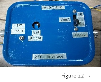
The circuit schematics for the operational attenuator/buffer and the current to voltage converter, are shown in Figure 21 and a photograph of the unit is shown as Figure 22.
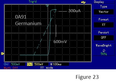
To test the system with something of similar conductivity and known provenance, an 0A91 diode was installed in the test assembly.
The resultant trace for the 0A91 diode is shown in figure 23; from which it may be observed that the forward current rises to 350uA at a voltage of approximately 200mV. Figure 23 certainly demonstrates the high conductivity of Germanium signal diodes!
An 'equivalent' trace for the Galena diode is shown in Figure 24 for comparison.
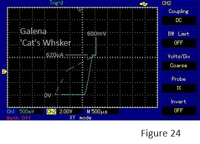
Unfortunately it was not noticed that the volts/division setting had inadvertently been changed relative to the setting employed to capture Figure 23* and in consequence the current rise displayed in Figure 24 is nearer to 700uA at a forward voltage of approximately 400mV so direct comparison is not practicable.
However, subject to the limitations of the measurement, the Galena signal diode appears to be as conductive as its Germanium counterpart.
However from a sharp transition to conduction, the slope appears to be perhaps more linear than that for the 0A91, which might explain the relatively lower distortion apparent in the demdulation test waveforms depicted in Figures 14 and 15.
* Easily done with a digital scope!
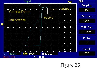
To complete the picture a characteristic for the Pyrites diode was acquired as shown in Figure 26 below:-
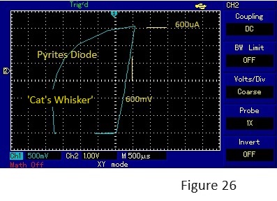
From Figure 26 it can be observed that the Pyrites 'Cats' Whisker' diode exhibited the abrupt turn on observed for its Galena counterpart and similar linearity but no amount of probing with the whisker resulted in conductivity equal to that exhibited by the latter in Figure 25.
It is astonishing that a semiconducting device discovered 100 years ago is so effective and which, in some aspects of performance, is superior to its successors.
In the very first paragraph of this rather long web page, I recorded that I had never built a traditional crystal set.
Consquently it was decided to have a go at making something which could have been constructed in the 1930s;
with an aim of making realistic comparisons between various crystal materials available at the time and subsequently. The arrangement shown in Figure 27 below was constructed accordingly . However the BBC has announced the termination of AM broadcasting in 2025 and consequently it is doubtful that that the aim will be fulfilled.
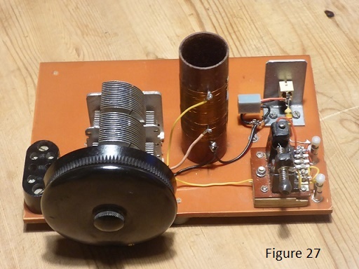
As shown, the arrangement is set up primarily for reception of the 198kHz BBC Radio 4 LW transmission but, with the addition of a two pole switch, it may be used for reception of local MW stations.
The terminal block on the left hand side of the srbp. chassis plate facilitates connection of the aerial wire and its earth (ground) counterpoise. A 50:1 Muirhead vernier drive for the tuning capacitor is a bit overkill in view of the Q factor achievable with an air cored inductor at 200kHz but if looks and feels good. The inductor, wound on an srbf. tube, comprises a LW coil tapped for aerial connectionl with faclity for use of the major portion to tune the MW with use of the above-mentioned switch.
On the rhs. of the chassis plate is the crystal detector assembly which embodies the 'cats whisker' arrangement used in foregoing tests but with additonal facility for shunting or bypasing this by an encapsulated diode provided by the spring terminals on the extreme right of the assembly.
An earphone jack socket is mounted behind the detector. Ideally high impedance (4000Ω) electro mechanical headphones should be used but good examples of these are becoming difficult to obtain and a crystal earpiece may be sustituted. Hearing aids preclude the use of the latter by the author and consequently the jack is primarily used for connection to a line amplifier and loudspeaker; which somewhat defeats the object of the exercise and makes crystal probing somewhat noisy!
Presently Radio 4 can be heard clearly using a 20m long aerial wire 2m from the ground but a higher and longer aerial would probably give better results. With the current arrangement, it might be concluded that the apparent sensitivity is slightly better with a probed Galena crystal detector than with an 0A90 Germanuim diode but a lot of probing and listening will be needed to confirm this.
Thanks for reading.
All information is free to use.