Back to Homepage & Index
As with the tunnel diode on page 19 of this website, another almost forgotten semiconductor device is the Unijunction Transistor.
It is difficult to believe that anyone set out to specifically develop the unijunction transistor and it is possible that it was a spin off from jfet. development.
An N type UJT. apparently comprises an N type silicon bar with an off-centre P diffusion into one side part way along its length, as is shown conceptually in Figure 1.
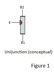
The bar has end connections labelled B1 and B2 and the heavily doped P region is closer to the B2 connection than it is to the B1 connection. The connection to the P region is called the Emitter. There is therefore only a single P-N junction, which is why the device is called a unijunction transistor.
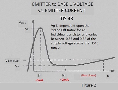
Like the tunnel diode on Page19, the unijunction transistor exhibits a negative resistance region in its forward conduction characteristic; making it suitable for use in very simple oscillator circuits. However it is not capable of operation at very high frequencies as is the tunnel diode and historically its most common application was the production of sawtooth waveforms for timebases etc. A typical characteristic of the type TIS43 UJT is shown in Figure 2.
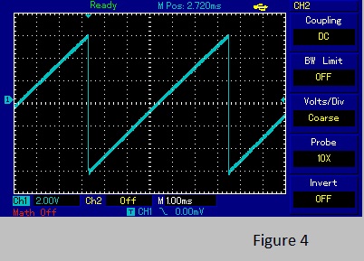
It can be seen from Figure 4 that the output at the emitter terminal is a linear ramp which rises approximately 12 Volts over 600us with a fall time (fly-back for a timebase) which is fast in comparison.
The reader might ask what occurs at terminals B2 and B1. The answer is 'not a lot' or more correctly a lot for a very short time.
As might be expected there is a negative going voltage transient at terminal B2 and a positive going one at terminal B1; which are the volt drops across their respective series resistors for the current flowing during the precipitous discharge of the capacitor connected to the emitter terminal.
The B2 and B1 waveforms are shown in Figure 5 and Figure 6 respectively.
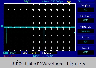
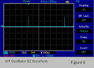
From these traces it appears that, during discharge, a current pulse of approximately 47mA flows into terminal B2 and a current of approximately 385mA flows from terminal B1 and that consequently the capacitor is discharged by a current of approximately 340mA into the Emitter terminal. Quite impressive considering that the power supply current limit was set to 20mA!
It might be expected that, should a negative going pulse be applied to terminal B2 prior to the discharge, the discharge can be started early i.e a timebase fly-back can be triggered; which is in fact the case.
Similarly the positive going excursion at terminal B1 might be applied to the cathode of a cathode ray tube
for fly-back blanking.
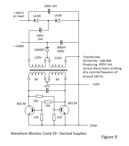
However it will be necessary to establish a power supply system for the for the 1CP1 crt. before timebase development can be undertaken. Also very conveniently a schematic of the tube requirements is published, free to use, by James Millen & Co and this is depicted in Figure 8; redrawn in accordance with my practice and components to hand. Thank you James Millen.
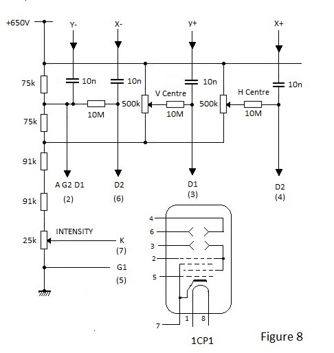
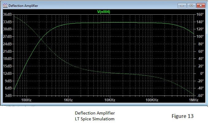
As can be seen, it is a simple differential amplifiier configured to permit output voltage swings of +/- 50V or so. Ac. coupling is employed with a low frequency cut off to reduce the response to mains frequency pick-up.
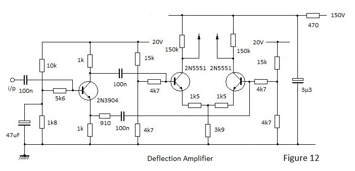
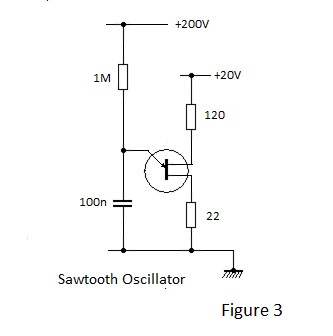
A timebase circuit having switched scan periods of 1s, 100ms and 10ms and based on the unijunction circuit of figure 3 is incorporated. This circuit includes a potentiometer which provides fine control (+/- 10% variation) of these periods. It is installed in the chassis but currently it cannot be used due to the existing capacitive coupling to the X amplifier and delection plates. What is required, and intended, is to convert to a negative supply for the cathode ray tube, thereby allowing the deflection plates to operate close to ground potential and thus to be directly connected. However the purpose of this page is to show a basic application of the unijunction transistor and further development of the monitor itself will not be recorded here.
All information is free to use.