An almost forgotten semiconductor device in this age of very small very fast transitors is the tunnel or Esaki diode.
Tunnel diodes became available in the early 1960s and they were capable of functioning at microwave frequencies albeit at very low power levels. Usually fabricated from Germanium, they were heavily doped with majority carriers to promote quantum tunnelling, characterised by very high conductance for low forward voltages.
However as the forward bias of a tunnel diode is increased its conductance progressively reduces to that of a 'normal' Germanium diode; presumably because insufficient tunnelling carriers are available to maintain such a high level of conductivity.
This phenomenon gives rise to a range of forward conduction over which current reduces with increasing voltage, i.e. a region of negative resistance.
In this region an oscillatory circuit, connected in series with the diode, will oscillate if its effective loss resistance is less than the incremental negative resistance of the diode characteristic.
Because the diode junction is heavily doped with majority carriers, minority carriers play no part in this action and the maximum frequency for oscillation is high.
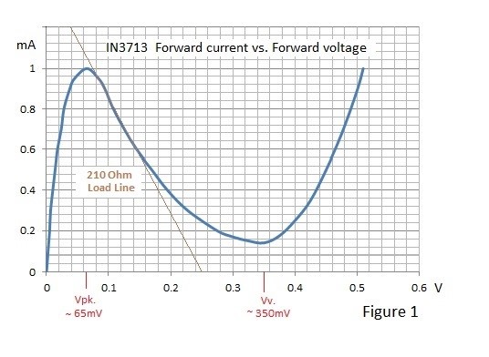
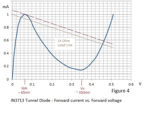
The General Electric IN3713 tunnel diode - the conduction characteristic for which is shown in Figure 1- will oscillate at frequencies up to 3.7 GHz. in a suitable circuit.
To operate as a monostable the load line must intercept the characteristic below the peak (or trigger) current of 1mA as shown in Figure 2; where a 250 Ohm load is shown operating from a supply of just over 200mV (Vbias).
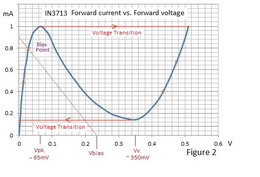
At this point the reader might conclude that the use of tunnel diodes in discrimiator circuits means working with output signals of less than 200mV amplitude. This is not the case because the diodes are current driven and and operating voltages are somewhat larger than would be the case with voltage drive.
Referring to Figure 2 it can be seen that with no additional current (signal current) the diode is biased below the 1mA peak trigger current on the positive resistance part of the characteristic so conditions are stable. However if a signal current increases the diode curent beyond the 1mA peak level the diode voltage will be in the unstable region of the characteristic and, in consequence, it 'leaps' to a higher and stable voltage of around 510mV.
When the signal current is removed current and voltage fall down the characteristic until the valley point of approximately 150uA and 350mV reached, where again instability is encountered. Consequently the voltage again leaps across to intersect the stable part of the charcteristic at a voltage of about 2.5mV from where it tracks the characteristic to the original stable bias current of 0.8mA with a forward voltage of approximately 42mV.
The locus of this operating path is shown in Figure 2 where transitions of approximately 500mV and 300mV are depicted by red arrows.
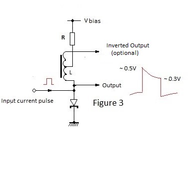
If the reduction of current and voltage to the valley point can be slowed by series inductance a 'wide' (long duration) voltage pulse can be be produced by the transition and it is here that the low resistance of the diode and its load come into play because low series resistance facilitates a relatively long L/R time constant with a given inductor slowing recovery and producing a voltage pulse as shown in Figure 3.
It is left to the reader to decide upon an application.
Ideally this page would be completed by a practical application of a Germanium tunnel diode and an attempt was made to procure a 1N3713 diode for this purpose. Fredcomponetes in Brazil stock 1N3713 diodes but they were unable to supply due to a Covid related embargo. Terry Tippett, with whom the author shares the Norcim site, also searched for a source of tunnel diodes and happened upon the site http://www.vk6fh.com/vk6fh/lambda_diode.htm describing a jfet complementary pair combination which exhibits negative resistance. The author has been fascinated by the concept of negative resistance since the days of thermionic valves but he had not heard of the the lambda diode.
The opportunity to investigate something fresh could not be resisted.
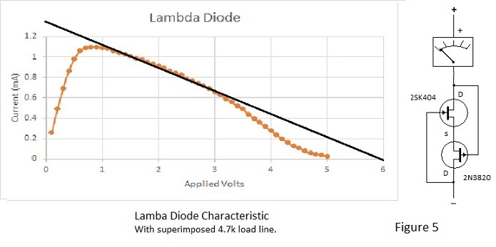
In its simplest form the lambda diode comprises an n jfet, p jfet pair coupled for mutual feedback as shown in Figure 5. Ideally these should be complementary pair but the device tested was assembled and from what was to hand; namely a 2SK404 n channel fet and a 2N3820 p channel fet as shown.
Having produced a Lambda diode it would be difficult not to test an application and, with this object, it was decided to investigate its operation in an oscillator circuit and to determine the working conditions for producing a clean sine wave at low radio frequency. The circuit shown in Figure 6 was constructed for this purpose.
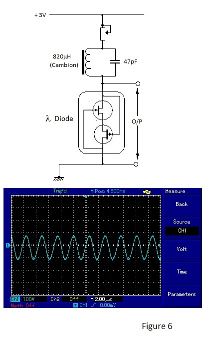
The circuit was found to oscllate readily and series resistance necessary to obtain a clean sine wave was determined by means of the variable resistor.
The resultant waveform, shown in the figure, was obtained operating from 3V supply with series resistance of 350Ω.
An LT Spice simulation for the condition resulting in the waveform shown in Figure 6 is shown in Figure 7.
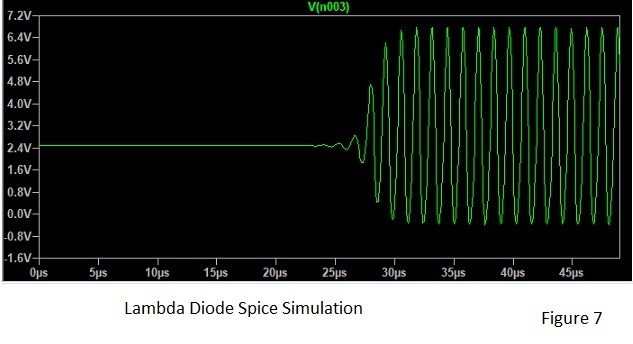
From Figure 7 It can be seen that the oscillation takes around 25us to build up from circuit noise.
With the variable resistor set to a lower value the build-up is more rapid at the expense of waveform purity.
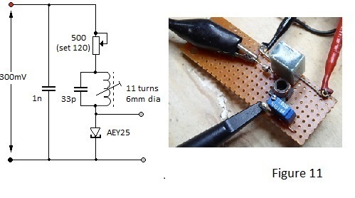
The aim of demonstrating an application of the 1N3713 tunnel diode being unfulfilled due to current non-availability, prompted the idea of trying something similiar.
An internet search indicated that the Mullard AEY25 tunnel diode is available from several sources; the main difference between the diodes being that the 1N3713 characteristic is specified to peak at 1mA and that for the AEY25 at 5mA. A couple of the latter were duly purchased for examination.
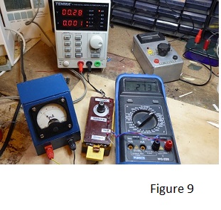
A complete forward conduction characteristic for the AEY25 device does not appear to be available so it was decided to determine the characteristic for one of the procured examples.
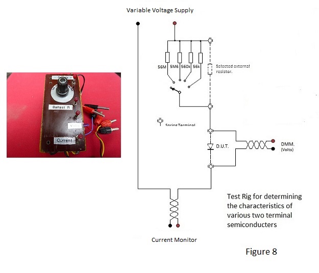
The test rig was connected to facilitate monitoring of forward voltage and current in the arrangement shown in Figure 9; where forward voltage is displayed
by a digital multi-meter and the current is measured using a moving coil milli-ammeter. (A predilection for oscillation in the negative resistance region of a tunnel diode characteristic causes difficulties with regard to the latter, which is the reason for the trio of graded capacitors across its terminals).
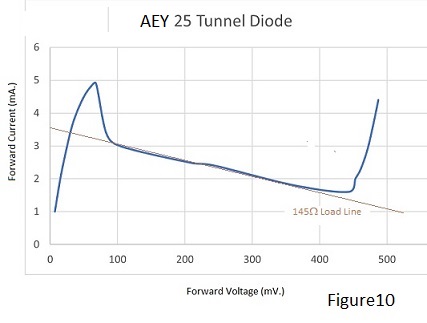
With the above arrangement the characteristic depicted in Figure 10 was obtained.
From Figure 10 it can be seen that,as expected, the current peaks at 5mA for an applied voltage of approximately 65mV.
Following a pronounced peak the current falls rapidly with increasing forward voltage, dropping to 3mA for an applied e.m.f. of approximately 100mV. following which the current falls quasi linearly with applied voltage to a minimum of around 1.5mA with an applied voltage of 400mV, creating a region of negative resistance with a slope equivalent to -145 Ohms. Following the region of negative resistance the relationship rapidly reverts to normal diode conduction.
With the object of facilitating the rapid plotting of the characteristics for "Cats Whisker" type contact detectors for Page 21 of this site, an ad.hoc. facility for diode curve tracing on an oscilloscope sceen was developed and it was decided to see what this made of the AEY25 tunnel diode reported upon in the foregoing paragraph.
Tunnel diodes are tricky beasts to test due to their proclivity for oscillation and testing involved the use of graded capacitors and ferrite beads.The trace obtained is shown in Figure 13 below. Current limiting, both positive and negative is not actual but it represents the limits of the current measuring circuit.
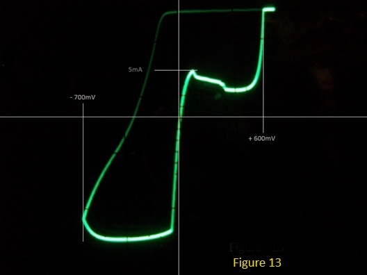
As may be seen from the figure, forward conduction is similar to that for the hand plotted charcteristic of Figure 10. What is perhaps unexpected is the reverse conduction. The hump on the haunch of the forward peak might well be low level oscillation, undisplayed as such due to the limited bandwidth of the oscilloscope used.
Tunnel diodes are indeed strange beasts.
Thank you for reading